- 您现在的位置:买卖IC网 > Sheet目录17367 > ISL85033EVAL2Z (Intersil)EVAL BOARD2 FOR ISL85033
�� �
�
�ISL85033�
�exponentially� increasing� with� temperature.� Due� to� the� nature� of�
�reverse� bias� leakage� vs� temperature,� the� diode� should� be�
�carefully� selected� to� operate� in� the� worst� case� circuit� conditions.�
�Catastrophic� failure� is� possible� if� the� diode� chosen� experiences�
�thermal� runaway� at� elevated� temperatures.� Please� refer� to�
�Application� Note� for� diode� selection.�
�Power� Derating� Characteristics�
�To� prevent� the� ISL85033� from� exceeding� the� maximum� junction�
�temperature,� some� thermal� analysis� is� required.� The�
�temperature� rise� is� given� by� Equation� 29:�
�can� degrade� efficiency,� radiate� noise� into� the� circuit,� and� lead� to�
�device� overvoltage� stress.� Careful� component� layout� and� printed�
�circuit� board� design� minimizes� these� voltage� spikes.�
�As� an� example,� consider� the� turn-off� transition� of� the� upper�
�MOSFET.� Prior� to� turn-off,� the� MOSFET� is� carrying� the� full� load�
�current.� During� turn-off,� current� stops� flowing� in� the� MOSFET� and�
�is� picked� up� by� the� Schottky� diode.� Any� parasitic� inductance� in�
�the� switched� current� path� generates� a� large� voltage� spike� during�
�the� switching� interval.� Careful� component� selection,� tight� layout�
�of� the� critical� components,� and� short,� wide� traces� minimizes� the�
�magnitude� of� voltage� spikes.�
�T� RISE� =� (� PD� )� (� θ� JA� )�
�(EQ.� 29)�
�There� are� two� sets� of� critical� components� in� the� ISL85033�
�where� PD� is� the� power� dissipated� by� the� regulator� and� θ� JA� is� the�
�thermal� resistance� from� the� junction� of� the� die� to� the� ambient�
�temperature.� The� junction� temperature,� T� J� ,� is� given� by�
�Equation� 30:�
�switching� converter.� The� switching� components� are� the� most�
�critical� because� they� switch� large� amounts� of� energy,� and�
�therefore� tend� to� generate� large� amounts� of� noise.� Next,� are� the�
�small� signal� components� which� connect� to� sensitive� nodes� or�
�supply� critical� bypass� current� and� signal� coupling.�
�T� J� =� (� T� A� +� T� RISE� )�
�(EQ.� 30)�
�A� multi-layer� printed� circuit� board� is� recommended.� Figure� 50�
�where� T� A� is� the� ambient� temperature.� For� the� QFN� package,� the�
�θ� JA� is� +38°C/W.�
�The� actual� junction� temperature� should� not� exceed� the� absolute�
�maximum� junction� temperature� of� +125°C� When� considering�
�the� thermal� design,� remember� to� consider� the� thermal� needs� of�
�the� rectifier� diode.�
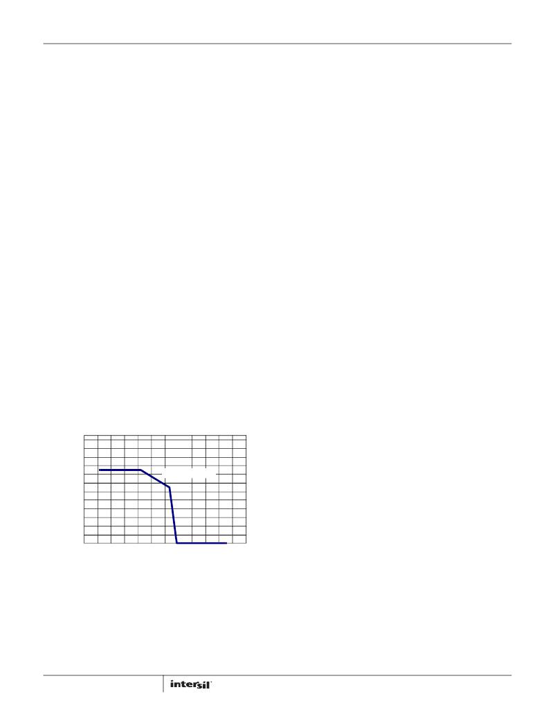
�The� ISL85033� delivers� full� current� at� ambient� temperatures� up�
�to� +85°C� if� the� thermal� impedance� from� the� thermal� pad�
�maintains� the� junction� temperature� below� the� thermal� shutdown�
�level,� depending� on� the� Input� Voltage/Output� Voltage�
�combination� and� the� switching� frequency.� The� device� power�
�dissipation� must� be� reduced� to� maintain� the� junction�
�temperature� at� or� below� the� thermal� shutdown� level.� Figure� 49�
�illustrates� the� power� derating� versus� ambient� temperature� for�
�the� ISL85033� EVAL� kit.� Note� that� the� EVAL� kit� derating� curve� is�
�based� on� total� circuit� dissipation,� not� IC� dissipation� alone.�
�120�
�110�
�100�
�90�
�shows� the� connections� of� the� critical� components� in� the�
�converter.� Note� that� capacitors� C� IN� and� C� OUT� could� each�
�represent� numerous� physical� capacitors.� Dedicate� one� solid�
�layer,� usually� a� middle� layer� of� the� PC� board,� for� a� ground� plane�
�and� make� all� critical� component� ground� connections� with� vias� to�
�this� layer.� Dedicate� another� solid� layer� as� a� power� plane� and�
�break� this� plane� into� smaller� islands� of� common� voltage� levels.�
�Keep� the� metal� runs� from� the� PHASE� terminals� to� the� output�
�inductor� short.� The� power� plane� should� support� the� input� power�
�and� output� power� nodes.� Use� copper� filled� polygons� on� the� top�
�and� bottom� circuit� layers� for� the� phase� nodes.� Use� the� remaining�
�printed� circuit� layers� for� small� signal� wiring.�
�In� order� to� dissipate� heat� generated� by� the� internal� LDO� and� MOSFET,�
�the� ground� pad� should� be� connected� to� the� internal� ground� plane�
�through� at� least� four� vias.� This� allows� the� heat� to� move� away� from� the� IC�
�and� also� ties� the� pad� to� the� ground� plane� through� a� low� impedance�
�path.�
�The� switching� components� should� be� placed� close� to� the�
�ISL85033� first.� Minimize� the� length� of� the� connections� between�
�the� input� capacitors,� C� IN� ,� and� the� power� switches� by� placing�
�them� nearby.� Position� both� the� ceramic� and� bulk� input� capacitors�
�80�
�70�
�60�
�50�
�Θ� JA� =� 38°C/W�
�as� close� to� the� upper� MOSFET� drain� as� possible.� Position� the�
�output� inductor� and� output� capacitors� between� the� upper� and�
�Schottky� diode� and� the� load.�
�40�
�30�
�20�
�10�
�0�
�0�
�1�
�2�
�3� 4� 5� 6� 7� 8� 9� 10�
�ISL85033EVAL1ZB� EVAL� BOARD�
�TOTAL� POWER� DISSIPATION� (W)�
�11�
�12�
�The� critical� small� signal� components� include� any� bypass�
�capacitors,� feedback� components,� and� compensation�
�components.� Place� the� PWM� converter� compensation�
�components� close� to� the� FB� and� COMP� pins.� The� feedback�
�resistors� should� be� located� as� close� as� possible� to� the� FB� pin� with�
�vias� tied� straight� to� the� ground� plane� as� required.�
�FIGURE� 49.� POWER� DERATING� CURVE�
�Layout� Considerations�
�Layout� is� very� important� in� high� frequency� switching� converter�
�design.� With� power� devices� switching� efficiently� between� 100kHz�
�and� 600kHz,� the� resulting� current� transitions� from� one� device� to�
�another� cause� voltage� spikes� across� the� interconnecting�
�impedances� and� parasitic� circuit� elements.� These� voltage� spikes�
�22�
�FN6676.6�
�February� 23,� 2012�
�发布紧急采购,3分钟左右您将得到回复。
相关PDF资料
MIC5891BWM
IC DRVR LATCH 8BIT SER IN 16SOIC
MIC5891BN
IC DRVR LATCH 8BIT SER IN 16DIP
TAAB336K010G
CAP TANT 33UF 10V 10% AXIAL
SPX385AS-L-1-2
IC VREF SHUNT PREC 1.235V 8SOICN
A9AAT-1105F
FLEX CABLE - AFE11T/AF11/AFE11T
TDC225K025NSE
CAP TANT 2.2UF 25V 10% RADIAL
MIC5841BWM TR
IC DRVR LATCH 8BIT SER IN 18SOIC
SPX432AM-L
IC VREF SHUNT PREC ADJ SOT-23-3
相关代理商/技术参数
ISL85033IRTZ
功能描述:IC REG BUCK SYNC ADJ 3A 28TQFN RoHS:是 类别:集成电路 (IC) >> PMIC - 稳压器 - DC DC 开关稳压器 系列:- 产品培训模块:Lead (SnPb) Finish for COTS
Obsolescence Mitigation Program 标准包装:2,500 系列:- 类型:降压(降压) 输出类型:两者兼有 输出数:1 输出电压:5V,1 V ~ 10 V 输入电压:3.5 V ~ 28 V PWM 型:电流模式 频率 - 开关:220kHz ~ 1MHz 电流 - 输出:600mA 同步整流器:无 工作温度:-40°C ~ 125°C 安装类型:表面贴装 封装/外壳:16-SSOP(0.154",3.90mm 宽) 包装:带卷 (TR) 供应商设备封装:16-QSOP
ISL85033IRTZ-T
功能描述:IC REG BUCK SYNC ADJ 3A 28TQFN RoHS:是 类别:集成电路 (IC) >> PMIC - 稳压器 - DC DC 开关稳压器 系列:- 产品培训模块:Lead (SnPb) Finish for COTS
Obsolescence Mitigation Program 标准包装:2,500 系列:- 类型:降压(降压) 输出类型:两者兼有 输出数:1 输出电压:5V,1 V ~ 10 V 输入电压:3.5 V ~ 28 V PWM 型:电流模式 频率 - 开关:220kHz ~ 1MHz 电流 - 输出:600mA 同步整流器:无 工作温度:-40°C ~ 125°C 安装类型:表面贴装 封装/外壳:16-SSOP(0.154",3.90mm 宽) 包装:带卷 (TR) 供应商设备封装:16-QSOP
ISL85033IRTZ-T7A
功能描述:直流/直流开关调节器 3A STD BUCK REG - 4X 4 TQFN 250 PC REEL RoHS:否 制造商:International Rectifier 最大输入电压:21 V 开关频率:1.5 MHz 输出电压:0.5 V to 0.86 V 输出电流:4 A 输出端数量: 最大工作温度: 安装风格:SMD/SMT 封装 / 箱体:PQFN 4 x 5
ISL8505IRZ
制造商:Intersil Corporation 功能描述:PB-FREE DC TO DC POWER SWITCHING, 38LD QFN 5X7 - Rail/Tube
ISL8510EVAL1Z
功能描述:EVALUATION BOARD FOR ISL8510 RoHS:是 类别:编程器,开发系统 >> 评估板 - DC/DC 与 AC/DC(离线)SMPS 系列:- 产品培训模块:Obsolescence Mitigation Program 标准包装:1 系列:True Shutdown™ 主要目的:DC/DC,步升 输出及类型:1,非隔离 功率 - 输出:- 输出电压:- 电流 - 输出:1A 输入电压:2.5 V ~ 5.5 V 稳压器拓扑结构:升压 频率 - 开关:3MHz 板类型:完全填充 已供物品:板 已用 IC / 零件:MAX8969
ISL8510IRZ
功能描述:IC REG DL BUCK/LINEAR 24-QFN RoHS:是 类别:集成电路 (IC) >> PMIC - 稳压器 - 线性 + 切换式 系列:- 标准包装:2,500 系列:- 拓扑:降压(降压)同步(3),线性(LDO)(2) 功能:任何功能 输出数:5 频率 - 开关:300kHz 电压/电流 - 输出 1:控制器 电压/电流 - 输出 2:控制器 电压/电流 - 输出 3:控制器 带 LED 驱动器:无 带监控器:无 带序列发生器:是 电源电压:5.6 V ~ 24 V 工作温度:-40°C ~ 85°C 安装类型:* 封装/外壳:* 供应商设备封装:* 包装:*
ISL8510IRZ-T
功能描述:IC REG DL BUCK/LINEAR 24-QFN RoHS:是 类别:集成电路 (IC) >> PMIC - 稳压器 - 线性 + 切换式 系列:- 标准包装:2,500 系列:- 拓扑:降压(降压)同步(3),线性(LDO)(2) 功能:任何功能 输出数:5 频率 - 开关:300kHz 电压/电流 - 输出 1:控制器 电压/电流 - 输出 2:控制器 电压/电流 - 输出 3:控制器 带 LED 驱动器:无 带监控器:无 带序列发生器:是 电源电压:5.6 V ~ 24 V 工作温度:-40°C ~ 85°C 安装类型:* 封装/外壳:* 供应商设备封装:* 包装:*
ISL85402EVAL1Z
制造商:Intersil Corporation 功能描述:ISL85402 EVAL BOARD1 - 20LD QFN - INPUT VOLTAGE 36V, 2.5A - Bulk